


Adani University AI Labs Open for New Engineering Skills
Adani University Opens Two Labs for AI and Engineering Learning
Adani University in Ahmedabad has added two new laboratories focused on artificial intelligence and engineering education, with support from Qualcomm Technologies and e-Yantra at IIT Bombay.
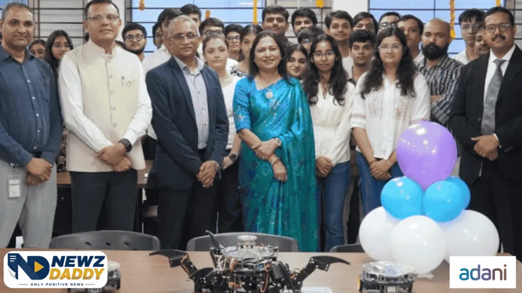
The Arduino Edge AI Lab, powered by Qualcomm Technologies, and the Engineering Exploration Program (EEP) Lab, developed with e-Yantra, IIT Bombay, were inaugurated on 6 July 2026. Dr Priti G. Adani, President of Adani University, opened the facilities in the presence of Rajen Vagadia, President of Qualcomm Technologies India.
The two labs are intended to give students more time working with hardware, software and engineering projects rather than learning only through classroom lessons. The work will cover areas such as Edge AI, Internet of Things (IoT), robotics, embedded systems, computer vision and automation.
For engineering students, the change is important because many of these technologies are now being used in products and industrial systems. AI is also moving beyond large data centres and cloud services. Smaller AI systems can process information on the device where it is collected. This is known as Edge AI.
Qualcomm’s current work with Arduino includes the Arduino UNO Q, a development board built around Qualcomm Dragonwing technology. It is designed to run AI applications on the device and can be used with Arduino App Lab for projects involving embedded systems, Linux and Edge AI. Qualcomm has also been running programmes that give students and developers practical experience with these tools.
At Adani University, the Arduino Edge AI Lab will allow students to build and test AI applications at the edge. Projects can involve connected devices, sensors, robots and computer vision systems.
The work also introduces students to problems that can be missed when AI is studied only through software. An AI device has to work within limits on power, memory, processing speed and heat. The university says students will work on these issues while designing and testing their projects.
The lab is also expected to be used for faculty training, student projects, applied research and prototypes. The possible areas listed by the university include smart IoT systems, industrial automation, robotics, computer vision, intelligent transport systems, healthcare technology, smart devices and connected systems.
The second facility takes a wider engineering approach. The EEP Lab, set up with e-Yantra, IIT Bombay, will provide practical training in electronics, programming, embedded systems, robotics and automation. Students will use experiments and projects to apply engineering principles to working models.
This approach fits the teaching model followed by e-Yantra. The programme is hosted by the Computer Science and Engineering department of IIT Bombay and funded by the Ministry of Education. Its stated focus is project-based learning, with students and teachers working with robotics and embedded systems to solve practical problems.
The scale of e-Yantra’s work also shows why such a laboratory can matter to engineering colleges. Its lab initiative currently reports more than 560 labs, over 2,660 colleges and more than 6,000 teachers engaged through its programmes. IIT Bombay has separately said the wider e-Yantra project has reached more than two lakh students and more than 3,200 institutes, with more than 590 labs established.
Adani University has already been using robotics and project work as part of its engineering activities. At its Drobotics Conclave in January 2026, Prof Kavi Arya of IIT Bombay spoke about the e-Yantra approach to building engineering skills through practical learning. The university’s robotics programme has also included student competitions involving autonomous robots, Arduino-based systems and maze-solving tasks.
The new laboratories bring these strands together. Students can work with electronic components and robots in the EEP Lab, while the Edge AI facility can take those projects towards systems that can sense, process information and respond locally.
For the university, the facilities also create a route for students and faculty members to work with industry experts on practical problems. The stated plan includes interdisciplinary projects, research and product development, with industry participation forming part of the learning process.
Provost Prof Dhaval Pujara said stronger links between universities and industry are needed to prepare graduates for a technology-led economy. He said exposure to current technologies and real engineering problems can help students develop practical skills, creativity and problem-solving ability.
Registrar Prof Amish Vyas said the laboratories would support applied research, projects involving more than one academic discipline and product development by students and faculty.
The timing also reflects a wider push towards hands-on AI and robotics education. In 2026, Qualcomm has been running developer and student activities around Edge AI, Arduino and robotics, including programmes that use the Arduino UNO Q and Qualcomm platforms for practical projects.
For students at Adani University, the immediate benefit will be access to equipment and project work inside the campus. The longer-term value will depend on how often the facilities are used, the quality of projects produced and whether those projects lead to useful research, prototypes or industry applications.
The two laboratories therefore mark a new addition to Adani University’s engineering facilities, with a clear focus on giving students practical experience in AI, electronics, robotics, embedded systems and connected technology.
Must Read:
Adani University MBA in Infrastructure Management Begins
Adani University Induction Programme 2026 Prepares Future Engineers